The GAA Revolution: How Gate-All-Around Transistors Are Redefining AI Chip Performance

After decades of dominance, the FinFET transistor architecture has reached its physical limits. As the semiconductor industry transitions to 2nm nodes and beyond, a fundamentally different approach is taking over: Gate-All-Around (GAA) transistors. This technology represents the most significant shift in chip manufacturing since the introduction of FinFETs themselves over a decade ago, and it's arriving just in time to fuel the AI revolution's insatiable appetite for computational power.
The End of the FinFET Era
For years, FinFET (Fin Field-Effect Transistor) technology enabled the continuation of Moore's Law, allowing chipmakers to cram more transistors into smaller spaces while maintaining power efficiency. But as feature sizes shrink below 3nm, the physics become unforgiving. Leakage current increases, gate control weakens, and the performance gains that once came reliably with each new node begin to diminish.
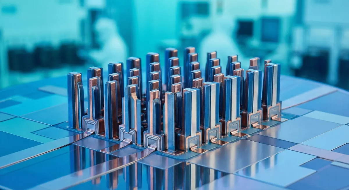
Enter Gate-All-Around transistors. Unlike FinFETs, which use vertical "fins" surrounded by gates on three sides, GAA transistors feature horizontal nanosheets completely encircled by the gate electrode. This 360-degree gate control delivers superior electrostatic performance, dramatically reducing leakage while boosting drive current and switching speed—exactly what AI workloads demand.
Mass Production Begins in 2026
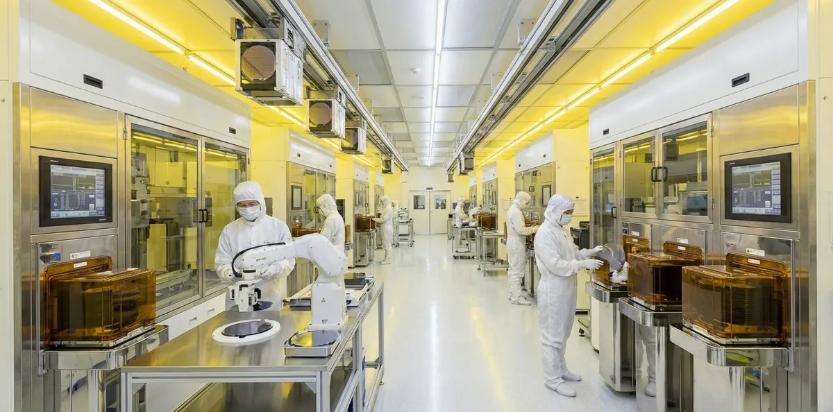
The transition from research lab to high-volume manufacturing is now underway. TSMC officially entered mass production of its N2 process—featuring GAA nanosheet transistors—in early 2026, with Apple and NVIDIA securing all initial capacity for upcoming iPhone 18 processors and next-generation AI accelerators. Samsung and Intel are following close behind with their own GAA implementations, marketed as MBCFET and RibbonFET respectively.
This convergence is no coincidence. The three foundry giants understand that success in GAA fabrication will determine who captures the lucrative AI hardware market over the next decade. With data center operators willing to pay premium prices for chips that can train and run ever-larger AI models, the stakes couldn't be higher.
Applied Materials Unveils Next-Generation Tools
As 2nm GAA chips ramp to volume, equipment manufacturers are already looking ahead. At SEMICON Korea last week, Applied Materials announced breakthrough innovations designed for angstrom-class nodes (sub-2nm), including:
- Applied Producer Viva: Performs ultra-pure radical channel treatments to reduce atomic-scale surface roughness, maximizing electron mobility in GAA nanosheets
- Molybdenum contacts: Replacing traditional tungsten contacts with molybdenum to improve conductivity and reduce resistance at the smallest scales
- Advanced interconnect systems: Enabling dense back-end wiring for 3D chip stacking and high-bandwidth memory integration
These tools address critical bottlenecks that emerge as transistors shrink toward atomic dimensions. Channel surface roughness, for instance, can scatter electrons and degrade performance—a problem that becomes catastrophic at 2nm and below. Applied's innovations aim to smooth these surfaces at the atomic level, preserving the mobility gains that GAA architecture promises.
Why GAA Matters for AI
AI workloads are uniquely demanding. Training large language models requires massive parallel computation across thousands of GPUs, while inference—running those models in production—demands both speed and energy efficiency at scale. GAA transistors deliver on both fronts:
- Higher performance: Improved gate control enables faster switching speeds and higher clock frequencies, directly translating to faster model training and inference
- Lower power consumption: Reduced leakage current means less wasted energy, critical for data centers already struggling with power density limits
- Better density: GAA's compact structure allows more transistors per square millimeter, increasing compute capacity without expanding chip size
These advantages compound in AI accelerators, where billions of transistors must work in concert to perform matrix multiplications and tensor operations. Even modest per-transistor improvements scale to substantial system-level gains when multiplied across an entire chip.
The Race to Angstrom Nodes
While 2nm represents a critical milestone, the industry isn't stopping there. TSMC, Samsung, and Intel have all announced roadmaps extending to 1.8nm, 1.4nm, and beyond—nodes measured in angstroms (tens of atoms) rather than nanometers. At these scales, traditional concepts of transistor design break down entirely, and GAA becomes the foundation for even more exotic architectures like Complementary FET (CFET) and Forksheet transistors.
The timeline is aggressive. TSMC's N2P (2nm Performance-enhanced) is slated for 2027, followed by N1.4 in 2028. Intel aims to reach its 14A (1.4nm-class) node by late 2027. Samsung is similarly pushing forward with its 1.4nm process. Each step requires not just shrinking existing structures, but rethinking how transistors are built, powered, and connected.
Supply Chain Implications
The GAA transition ripples through the entire semiconductor supply chain. Equipment manufacturers like Applied Materials, ASML, and Tokyo Electron are investing billions in next-generation lithography, deposition, and etching tools. Materials suppliers are developing new high-k dielectrics and metal gate materials optimized for GAA structures. And fabless chip designers are overhauling their design flows to exploit GAA's unique characteristics.
The financial commitment is staggering. A single leading-edge fab now costs upwards of $20 billion to build and equip, with much of that investment going toward advanced GAA-compatible tooling. This capital intensity is consolidating the industry, leaving only the largest and best-funded players capable of competing at the cutting edge.
Challenges Ahead
Despite its promise, GAA fabrication is extraordinarily difficult. The nanosheet structures require atomic-precision control during epitaxial growth, with thickness uniformity measured in single-digit angstroms. Any variation can lead to performance mismatches and yield loss. Process integration is equally challenging—stacking multiple nanosheet layers while maintaining electrical isolation and thermal performance pushes the limits of current manufacturing capabilities.
Cost is another concern. Early 2nm wafers are expensive, with per-chip costs potentially 20-30% higher than equivalent 3nm parts. As yields improve and production scales, these premiums should shrink, but the economics will pressure chipmakers to reserve GAA processes for high-value products: flagship smartphones, premium GPUs, and AI accelerators where performance justifies the expense.
The Broader Context: AI's Silicon Hunger
GAA's arrival couldn't be better timed. The AI boom shows no signs of slowing, and every major tech company is racing to deploy larger, more capable models. GPT-5, Gemini Ultra, Claude Opus—each generation demands exponentially more compute. Without architectural leaps like GAA, the industry would hit a wall where power and heat constraints make further scaling impossible.
This is the "AI Giga-Cycle" that industry analysts describe: a multi-year period where semiconductor demand is driven not by incremental smartphone upgrades or modest server refresh cycles, but by a fundamental restructuring of computing infrastructure around AI workloads. GAA is the enabling technology making this cycle possible.
Looking Forward
As 2026 unfolds, the semiconductor industry is entering uncharted territory. The physics at 2nm and below defy many traditional assumptions, and success will require not just better tools and materials, but entirely new ways of thinking about transistor design. GAA is a solution, but it's also a stepping stone toward even more radical architectures that may define the post-2nm era.
For now, the focus is on execution. TSMC, Samsung, and Intel are locked in a high-stakes race where stumbling could mean ceding market leadership for years. Equipment suppliers are sprinting to deliver next-generation tools. And chip designers are learning to harness GAA's unique properties to squeeze every last drop of performance from these atomic-scale structures.
The GAA revolution is underway. The chips powering tomorrow's AI systems are being manufactured today, one nanosheet at a time.
Related Articles
TSMC Enters the 2nm Era: Apple and NVIDIA Lock Up All Initial Capacity
TSMC began 2nm N2 mass production with GAAFET technology. Apple and NVIDIA reserved 100% of initial capacity.

The GPU Wars Heat Up: Custom Silicon Takes Center Stage
Major tech companies are designing custom AI accelerators to reduce dependence on NVIDIA's dominance.

The AI Power Crisis: Data Centers Strain Electrical Grids Worldwide
AI workloads are pushing data center power consumption to unprecedented levels, forcing infrastructure rethinks.