Breaking: Nvidia is about to do something it has never done before — publicly admit that its GPUs aren't the best tool for every AI job. According to a WSJ report published February 28th and corroborated by Reuters, Nvidia will unveil a radical new inference-focused processor at GTC 2026 (March 16–19, San Jose) that incorporates technology from startup Groq — a company Nvidia quietly paid $20 billion to license in late 2025. OpenAI has already signed on as one of the platform's largest customers. The implications are seismic.
Why This Moment Is Different
For three years, Nvidia CEO Jensen Huang has insisted that the company's flagship GPUs — from Hopper to Blackwell to the just-entering-production Vera Rubin — are best-in-class for both AI training and AI inference. That claim was credible when training dominated AI compute budgets. It's crumbling fast now that inference does.
The math is unforgiving. Training a frontier model like GPT-5 or Gemini Ultra happens once (or a handful of times). Inference — answering every user query, powering every AI agent, running every background reasoning task — happens billions of times per day. As agentic AI explodes across enterprise software, coding tools, and consumer apps, the inference load is doubling roughly every three to four months. And GPUs, it turns out, are expensive, power-hungry, and architecturally over-engineered for this specific workload.
OpenAI has been one of the loudest voices making this case internally. Reuters reported in February that the ChatGPT maker was "unsatisfied with the speed at which Nvidia's hardware can spit out answers" for key workloads including software development and multi-agent orchestration. OpenAI began shopping for alternatives — talking to Cerebras, to Groq directly, even exploring Amazon's Trainium silicon. Then Nvidia made a move that shut those conversations down.
The $20 Billion Groq Acquisition That Nobody Fully Understood — Until Now
In December 2025, Nvidia announced what it called a "licensing deal" with Groq — a Silicon Valley startup founded in 2016 by Jonathan Ross, one of the architects of Google's original TPU chips. The headline number was $20 billion, making it the largest deal Nvidia has ever done. Nvidia also hired Groq's top leadership, including Ross, in what Silicon Valley immediately recognized as an "acqui-hire" of the company's most valuable intellectual property.
At the time, many analysts were puzzled. Groq's Language Processing Unit (LPU) was fast, sure — the company had benchmarks showing it generating tokens at 500+ tokens per second, roughly 10x faster than comparably sized Nvidia GPUs for pure inference throughput on large language models. But Groq's revenue was modest, its manufacturing was fabless (relying on TSMC), and its customer base was primarily developers using its cloud API. Why pay $20 billion for a company that size?
The answer, now clear, is that Nvidia wasn't buying Groq's business. It was buying Groq's architecture — and using it to plug a genuine gap in its product lineup before competitors like Cerebras, Amazon, and Google could exploit that gap to full effect.
What Makes Groq's LPU So Different from a GPU
To understand why this matters, you need to understand why GPUs aren't ideal for inference in the first place.
GPUs were designed for parallel workloads — doing millions of similar calculations simultaneously. That's perfect for training, where you're computing gradients across billions of parameters in parallel batches. But inference for large language models is fundamentally sequential: you generate one token, feed it back into the model, generate the next token, and so on. The bottleneck isn't raw compute — it's memory bandwidth and latency. The model weights need to move from memory to compute units constantly, and HBM (high-bandwidth memory) stacks, even at their best, can't keep up with the pace a pure inference chip demands.
Groq's LPU solves this with a radically different architectural philosophy:
- Hundreds of megabytes of on-chip SRAM as primary weight storage — not cache, but the actual memory where model weights live. This eliminates the DRAM/HBM bandwidth bottleneck entirely for models small enough to fit on-chip.
- Deterministic execution — unlike a GPU's complex scheduling and memory hierarchies that introduce variable latency, the LPU uses what Groq calls a "programmable assembly line" architecture. The compiler knows exactly when data will arrive at each computation stage. No stalls, no cache misses, no unpredictable delays.
- SIMD (Single Instruction, Multiple Data) optimization for transformer attention patterns — the dominant compute pattern in modern LLMs — with hardware that maps precisely to that pattern instead of treating it as a general-purpose workload.
The result: dramatically lower latency (time-to-first-token), dramatically lower energy consumption per token, and dramatically lower cost per million tokens compared to running the same model on Nvidia's H100 or B200 GPUs — at least for the inference-only use case.
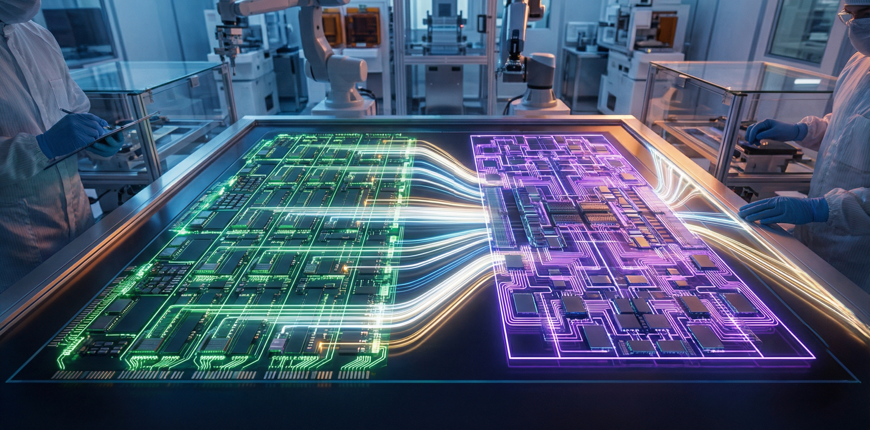
Enter Feynman: Nvidia's Hybrid Inference Platform
What Nvidia is building for GTC 2026 isn't a straight LPU. It's a hybrid platform — and the architecture being discussed in industry circles goes by the codename Feynman, named after the legendary physicist Richard Feynman (Nvidia has a tradition of naming architectures after scientific pioneers: Hopper, Ampere, Volta, Turing).
Based on what's emerged from supply chain sources and industry analysts in the weeks leading up to GTC, the Feynman platform appears to have several distinctive characteristics:
- 3D stacking of LPU elements with conventional compute — using advanced packaging (likely TSMC's CoWoS-S or a next-generation variant) to physically integrate Groq-derived inference logic with Nvidia's GPU cores in the same package. This allows the chip to dynamically route workloads: training or batched inference goes to the GPU cores; low-latency sequential inference goes to the LPU section.
- Massively expanded on-chip SRAM — early reports suggest Feynman may carry several hundred megabytes of SRAM integrated at the die level, enough to hold smaller fine-tuned models (7B to 70B parameters in quantized form) entirely on-chip for near-zero-latency responses.
- Targeting TSMC's 1.6nm A16 process — which would make Feynman among the first chips in production on the most advanced node in the industry, offering significant power efficiency improvements over Blackwell's N4P process.
- HBM4 memory interface — for the larger-model inference workloads that can't fit on-chip SRAM, Feynman will use HBM4 for higher bandwidth than anything currently shipping.
Jensen Huang has been notably cryptic about GTC 2026, telling press it will feature a reveal "meant to surprise the world." For a man who has announced trillion-parameter model training clusters and six-chip supercomputers with apparent equanimity, that's a high bar of intentional hype.
OpenAI's Role: From Dissatisfied Customer to Launch Partner
The business story here is as striking as the technical one. OpenAI spent the better part of Q4 2025 and early Q1 2026 publicly and privately lobbying for alternatives to Nvidia silicon. The company signed a multibillion-dollar partnership with Cerebras — whose Wafer Scale Engine 3 offers competitive inference speeds. It was in active negotiations with Groq directly. It announced it would use Amazon's Trainium chips for certain workloads.
Then Nvidia's $20 billion Groq licensing deal removed Groq from the table as an independent option. And OpenAI, which had been angling to play chipmakers off against each other to lower costs, found itself in a different negotiating posture.
According to sources cited by the WSJ, OpenAI has now agreed to become one of the largest customers of Nvidia's new inference platform — and Nvidia simultaneously announced a $30 billion investment in OpenAI alongside a "dedicated inference capacity" purchase agreement. This is a remarkable full-circle: OpenAI's push for inference alternatives essentially catalyzed Nvidia building the inference chip it needed, which OpenAI is now buying at scale.
The deal also signals something about Nvidia's strategic posture: the company is increasingly willing to take equity stakes in its customers, effectively creating vertically integrated AI compute-plus-application relationships that lock in long-term revenue while giving it intelligence on where the market is heading.
The Competitive Landscape This Reshapes
Nvidia's inference move doesn't arrive in a vacuum. The inference chip space has been one of the most competitive in semiconductors for the past eighteen months:
Google's TPU v6 (Trillium) remains the gold standard for inference on Gemini models, and Google uses it to serve Search AI features at scale. But it's largely proprietary — Google Cloud customers can access it, but there's no off-the-shelf product.
Amazon's Trainium2 and Inferentia3 are increasingly credible, and AWS has been aggressively pushing them as cost-effective alternatives. OpenAI's deal to use Trainium chips was the clearest signal yet that even Nvidia's largest customers are willing to diversify.
Cerebras WSE-3 is the most extreme inference-focused chip on the market — a single wafer-scale die with 900,000 AI cores and 44GB of on-chip SRAM. Cerebras CEO Andrew Feldman has not been shy about claiming it outperforms Nvidia for inference latency. OpenAI's Cerebras partnership pre-dates the Nvidia inference announcement, and Cerebras is unlikely to be displaced entirely.
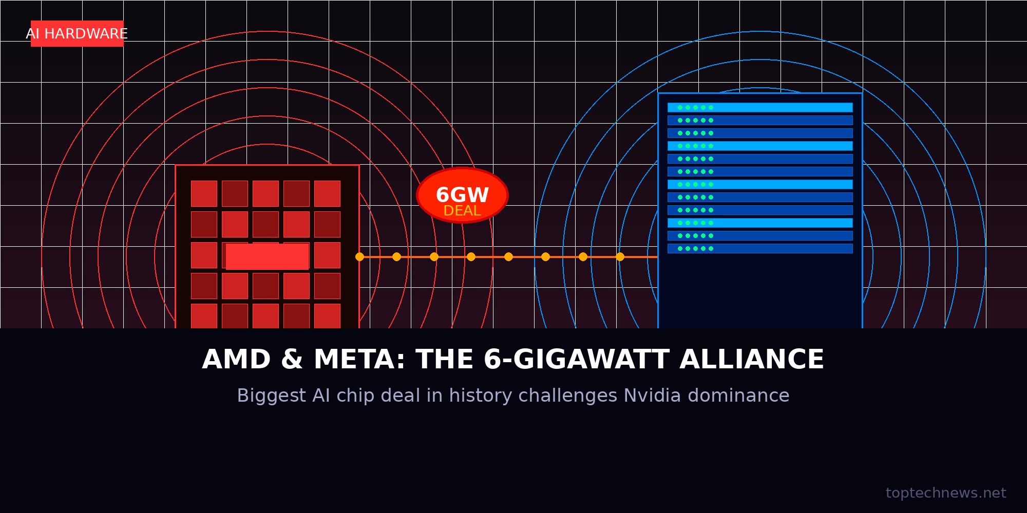
AMD's MI450 is a credible training competitor but has made less headway on pure inference performance claims. The Meta 6-gigawatt deal announced last week is primarily for training and fine-tuning workloads.
Where does a Nvidia Feynman platform fit in this landscape? If the technical specifications hold — and if Nvidia can deliver the manufacturing ramp on TSMC A16 without the yield issues that have haunted other cutting-edge node launches — it potentially offers what none of the alternatives currently provide: a single platform that handles training, batched inference, and ultra-low-latency agentic inference workloads at hyperscale. That's Nvidia's core value proposition: CUDA compatibility, ecosystem depth, and now architectural versatility.
What Agentic AI Demands That Current Hardware Can't Deliver
The underlying driver of all this activity is worth examining directly: the rise of agentic AI.
Training an AI model is a batch process — you run it once, over days or weeks, on the largest cluster you can afford. Inference for chatbots is a batch-friendly process too — you serve thousands of users simultaneously with each GPU, amortizing costs across the batch. But agentic AI — systems that autonomously plan, reason, write code, execute tools, and loop back on their outputs — is fundamentally different. Agents need:
- Ultra-low latency per reasoning step, because they chain dozens or hundreds of model calls to complete a single task
- High throughput at small batch sizes, because each agent instance runs mostly independently rather than in neat, batchable parallel streams
- Energy efficiency, because agent workloads run continuously rather than in discrete user sessions
- Cost per token at the floor, because agentic workflows can generate 10–100x more tokens per user task than simple Q&A
GPU hardware — optimized for large-batch, high-throughput workloads — struggles with the first two. An H100 serving a single agent reasoning chain is massively underutilized. This is exactly the problem Groq's LPU was designed to solve, and exactly why Nvidia paid $20 billion to integrate it.
The industry's ability to deploy AI agents at scale — not just in research demos but in production enterprise workflows — may ultimately hinge on whether chips like Feynman can close the cost and latency gap to make agentic compute economically viable at the unit level.
Manufacturing Risk: The TSMC A16 Wildcard
There is a significant wildcard in this story: manufacturing. TSMC's A16 process node (1.6nm-class) is on a tight production ramp. The node introduces backside power delivery for the first time in TSMC's mainstream lineup — a technology that improves power efficiency substantially but adds process complexity. Early yield rates on a new, complex node are historically challenging.
Nvidia's Blackwell B100 launch saw supply-side delays related to CoWoS packaging capacity rather than die yield — a cautionary tale about how cutting-edge packaging constraints can bottleneck even mature chip designs. Feynman, if it uses 3D stacking of heterogeneous dies on A16, faces both node yield and packaging complexity simultaneously.
This is one reason analysts are watching Jensen Huang's GTC keynote language carefully. A "reveal" can mean anything from a working silicon demo to a PowerPoint roadmap. The distinction will matter enormously to customers planning infrastructure deployments for 2027 and beyond.
The DeepSeek Dimension: Why Inference Efficiency Has Never Mattered More
One more thread in this story: DeepSeek. The Chinese AI lab stunned the industry in January with its R1 model — achieving near-frontier performance at a tiny fraction of the training cost, primarily through inference-time computation techniques like chain-of-thought reasoning and mixture-of-experts architecture. Reuters reported this week that DeepSeek has withheld its latest model from Nvidia and AMD, giving Huawei and Chinese chipmakers a multi-week head start to optimize their software stack.
DeepSeek's architectural innovations — particularly its emphasis on inference-time "thinking" as a substitute for brute-force training scale — validate everything Nvidia is doing with Feynman. If the industry trend moves toward models that "think more at inference time" rather than "train on more data," then inference hardware efficiency becomes the most critical competitive variable in AI computing. Nvidia, with a $20 billion bet on Groq's LPU technology, is making exactly that bet.
Bottom Line: The Shape of AI Hardware in 2027
Here's what all of this suggests about the near-term hardware landscape:
Nvidia's GPU monopoly is evolving, not ending. The company is expanding its platform to capture the inference market rather than ceding it. The $20B Groq deal and Feynman aren't admissions of GPU weakness — they're a strategic land-grab of an adjacent market before competitors can establish lasting footholds.
The inference chip market is bifurcating. Ultra-large models (>100B parameters, like GPT-5 class) will likely continue to need GPU-class compute even for inference — because the sheer parameter count demands the HBM bandwidth that LPUs lack. Smaller, fine-tuned, specialized models (7B–70B) run better on LPU-style chips. Feynman's hybrid approach may be the first platform that handles both credibly.
OpenAI's chip strategy is a hedge, not a commitment. The company is simultaneously using Cerebras, Amazon Trainium, and now Nvidia's inference platform. This reflects the reality that different workloads favor different silicon, and no single vendor has the complete solution.
GTC 2026 on March 16 is must-watch. Jensen Huang's keynote has the potential to be the most significant hardware announcement since the original Blackwell reveal at GTC 2024. If Feynman delivers on what the leaks suggest, it could reset competitive dynamics across the entire AI compute industry — and validate Nvidia's audacious $20B bet on Groq's decade-old architectural insight.
The age of GPU-only AI is ending. What comes next will be defined in San Jose, in fifteen days.