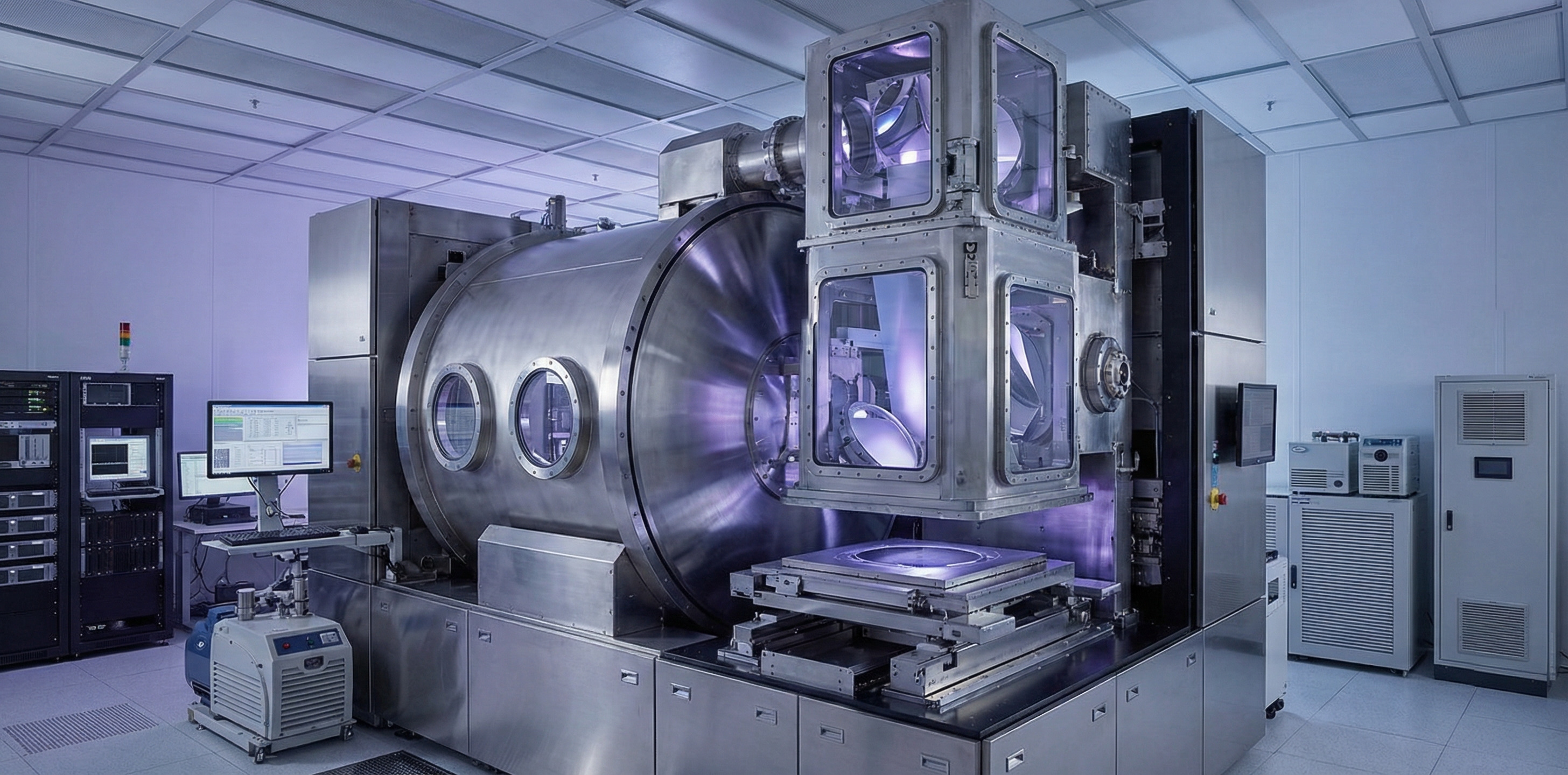
After years of painstaking development and billions in R&D spending, ASML has announced that its next-generation High-NA EUV lithography machines are ready for high-volume chip production — a pivotal milestone that removes the last significant technical barrier between today's AI chips and the denser, more efficient silicon the industry desperately needs. The announcement, made by ASML's Chief Technology Officer Marco Pieters at a technical conference in San Jose on February 26, arrives just as the AI industry's appetite for processing power has begun to outpace what current manufacturing tools can reliably produce.
The Machine Behind Every AI Chip You've Never Heard Of
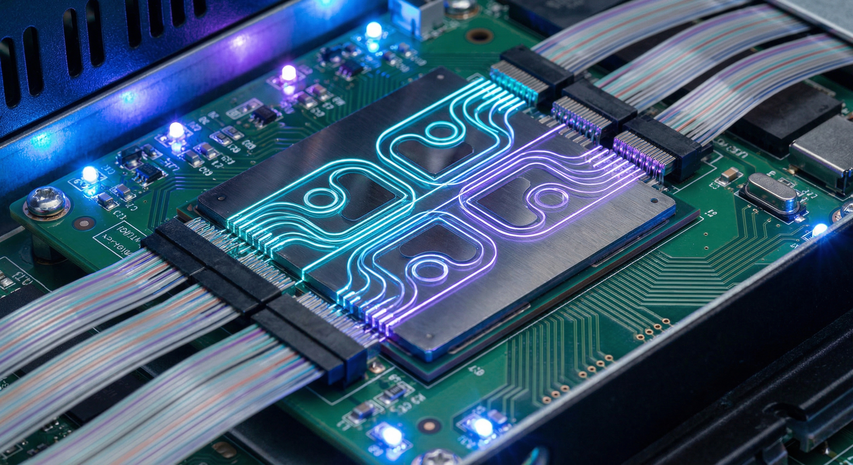
ASML operates in a strange position in the semiconductor ecosystem. It doesn't make chips — it makes the machines that make chips. And yet, without ASML, none of the world's most advanced AI silicon could exist. The Dutch company is the sole commercial manufacturer of extreme ultraviolet (EUV) lithography systems, the tools that print microscopic circuit patterns onto silicon wafers using light with wavelengths shorter than a nanometer. No other company in the world has successfully replicated this technology at commercial scale.
Lithography is the heartbeat of semiconductor manufacturing. The shorter the wavelength of light used, the finer the features that can be printed — which translates directly into smaller transistors, more of them per chip, and lower power consumption per operation. Current-generation EUV machines, which use light at a wavelength of 13.5 nanometers, have driven the industry from 7nm chips to today's 3nm and 2nm nodes. But those machines are now approaching their technical limits, according to ASML's own data. To go further — to build the AI chips of 2027, 2028, and beyond — the industry needs something new.
That something new is High-NA EUV.
What High-NA EUV Actually Does
The "NA" in High-NA EUV stands for numerical aperture, a measure of the angular range of light that a lens can capture and focus. A higher numerical aperture allows finer resolution — meaning the tool can print smaller features more accurately. ASML's current EUV machines operate at NA 0.33. The new High-NA systems push that figure to 0.55, a nearly 70% increase in optical resolution that opens up feature sizes impossible to achieve with the existing generation of tools.
More importantly, High-NA EUV allows chipmakers to collapse multiple processing steps into one. Under the current regime, achieving sub-2nm feature densities requires chipmakers like TSMC and Intel to run wafers through EUV machines multiple times — a process called multi-patterning that adds cost, time, and opportunities for error. ASML's new data, which Pieters disclosed in San Jose, shows that a single High-NA pass can replace several older-generation EUV steps, compressing the process and improving yield simultaneously.
The economic implication is substantial. High-NA EUV machines are extraordinarily expensive — each system costs well in excess of $300 million and requires months to install and calibrate. But if a single High-NA pass genuinely replaces three or four conventional EUV steps, the total cost calculus can favor the new machines despite their sticker price, particularly for chipmakers running the most advanced nodes at the highest volumes.
500,000 Wafers and Climbing
ASML's confidence in announcing production readiness isn't rhetorical — it's backed by process data. The company disclosed that its High-NA systems have now processed 500,000 wafers in development and qualification work, providing a statistically robust picture of machine performance, defect rates, and throughput consistency.
Current uptime sits at approximately 80%, and ASML is targeting 90% by the end of 2026. That number matters enormously in semiconductor manufacturing, where machine availability translates directly to factory output and revenue. A machine that runs 90% of the time versus 80% effectively represents a 12.5% capacity increase per installed unit — a significant buffer as chipmakers plan their capital expenditure programs.
CTO Marco Pieters was careful to temper expectations on deployment timelines. Full integration of High-NA EUV into high-volume manufacturing is expected to take two to three years, meaning the first production chips built with these tools are more likely to arrive in 2028 or 2029 than tomorrow. But the announcement of readiness is the critical gate: chipmakers can now begin the serious qualification work required before committing production lines to a new tool generation.
Why TSMC and Intel Are Watching Closely
The two chipmakers with the most at stake are TSMC and Intel, both of which have publicly committed to manufacturing nodes that depend on High-NA EUV technology.
TSMC's roadmap extends beyond its current N2 (2nm) node toward A16 (1.6nm) and eventually sub-angstrom densities. Each step down that ladder requires the resolution capabilities that only High-NA EUV can provide. Taiwan Semiconductor has been an early ASML customer for the new machines and has been quietly running qualification work for months. The production readiness announcement accelerates their path to full adoption.
Intel's situation is more complicated. The company's Intel 18A process node, which it has positioned as the cornerstone of its foundry business revival, already relies on EUV at multiple steps. Moving to High-NA EUV for future nodes (Intel 14A and beyond) is central to Intel's competitive strategy against TSMC. The readiness news is positive for Intel's long-term foundry ambitions, though Intel's near-term challenges are more financial and organizational than lithographic.
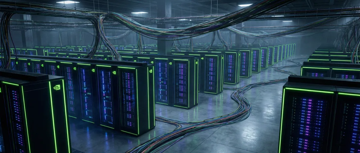
For the AI chip industry broadly, the implications flow through both companies. NVIDIA designs its leading-edge GPUs at TSMC. AMD does the same. As long as TSMC's roadmap advances, the performance trajectory of AI silicon continues. High-NA EUV is what makes that advancement physically possible.
Beyond EUV: ASML's Bigger Ambition
In a separate Reuters exclusive published on March 2nd — just days after the High-NA announcement — ASML's CTO outlined a broader strategic vision that extends well beyond lithography itself.
The company is moving into advanced packaging, the market for tools that bond, stack, and interconnect multiple specialized chips into a single system. This is a fast-growing segment of semiconductor manufacturing driven by the same AI demand that is filling ASML's order books. As AI chips increasingly rely on chiplet architectures — packaging separate logic, memory, and I/O dies together rather than monolithically integrating them — the tooling for that interconnection becomes a critical part of the manufacturing stack.
Advanced packaging is already a multi-billion-dollar market dominated by players like Tokyo Electron, Applied Materials, and BESI. ASML entering this space with its brand equity, customer relationships, and engineering depth represents a meaningful competitive disruption. Pieters framed it as a logical extension: "We look, not just for the next five years, we look at the next 10, maybe 15 years," he told Reuters. "What are potential directions the industry could take, and what would it require in terms of packaging, bonding, etc.?"
The company is also exploring whether it can expand the maximum size of chips it can print beyond the current limit — approximately the footprint of a postage stamp — which constrains the physical dimensions of die designs and limits throughput per wafer pass. A larger printable field would allow chipmakers to explore die designs currently impossible to manufacture, or to run multiple smaller dies per exposure with greater flexibility.
The AI-in-the-Machine Angle
There is a recursive quality to ASML's plans that is worth noting. The same AI systems that depend on ASML's machines for their silicon are now being incorporated into those machines to improve their performance. Pieters disclosed that ASML intends to deploy AI to accelerate the control software for its lithography systems and to speed up in-process chip inspection — the real-time quality verification that flags defects during a production run.
This is not a peripheral detail. EUV machine control software is extraordinarily complex, managing plasma light sources, mirror alignment systems measured in picometers, and wafer stage positioning that must remain accurate to fractions of a nanometer across thousands of cycles per hour. Any meaningful acceleration in that software improves throughput and reduces defect rates. Using AI to optimize what are currently hand-tuned control loops could yield meaningful manufacturing gains without requiring new hardware generations.
The Geopolitical Undercurrent
No ASML story in 2026 is complete without acknowledging the geopolitical context that surrounds every machine the company ships. The Dutch government, under sustained pressure from Washington, has maintained export restrictions that prevent ASML from delivering its most advanced EUV systems — and certainly High-NA EUV — to Chinese chipmakers. This has been a persistent source of tension for ASML, which had significant revenues from Chinese customers before the restrictions tightened.
The High-NA production readiness announcement effectively widens that gap. As TSMC, Intel, and Samsung begin the integration work that will embed High-NA EUV in their most advanced production lines, Chinese chipmakers — even well-funded state-backed players like SMIC — will remain at least one full node generation behind, locked out of the tooling that would allow them to close the distance. This is precisely the outcome U.S. and allied export policy was designed to achieve, and the ASML milestone locks it in for years.
There is a third generation of EUV already in research at ASML, though the company has provided few technical specifics. The trajectory is clear: each generation of EUV technology extends ASML's monopoly and deepens the advantage held by the handful of chipmakers with access to the machines. For the AI industry, that concentration of capability is both an asset — it creates predictable, ever-improving silicon — and a risk, since any disruption at ASML propagates through the entire global AI hardware supply chain within months.
What Comes After
The 2-3 year integration timeline Pieters outlined should be read as a floor, not a ceiling. Semiconductor manufacturing transitions are historically slower than announced, with qualification data, yield ramp challenges, and supply chain constraints conspiring to push schedules right. The first High-NA EUV production chips will likely appear in leading AI hardware around 2028-2029 — coinciding, roughly, with NVIDIA's expected post-Rubin architecture and TSMC's A14 node.
What that silicon looks like is already being designed. The process engineers at TSMC and Intel are working now, in advance of High-NA volume availability, on layouts optimized for the new tool's optical characteristics. The chip architectures NVIDIA, AMD, and custom silicon teams at Google, Amazon, and Apple will run on those processes are in early stages of development. The ASML announcement in San Jose wasn't just a manufacturing milestone — it was the opening of a planning window that stretches to the end of the decade.
For the AI industry, a roadmap that extends reliably to 2030 is an extraordinary asset. The machines that will run those models are being designed today, in large part, on the assumption that ASML delivers. Last week in San Jose, the company confirmed that assumption is still sound.