TSMC's groundbreaking 2-nanometer process technology entered mass production in late 2025, and the industry's largest technology companies are already fighting for every available wafer. With capacity sold out through late 2026 and revolutionary backside power delivery on the horizon, the race for silicon supremacy has never been more intense—or more critical for the future of AI.
The Launch: TSMC Enters the GAA Era
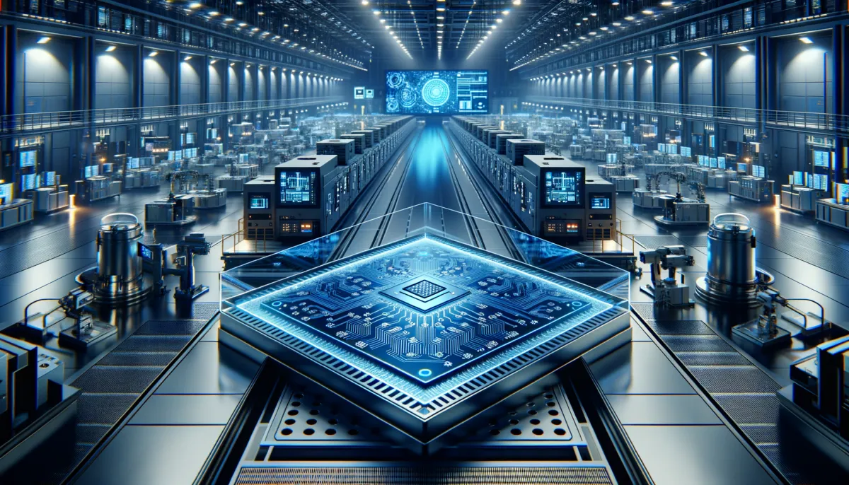
Taiwan Semiconductor Manufacturing Company (TSMC) crossed a critical threshold in December 2025 when it began volume production of its N2 process node—marking the company's first deployment of gate-all-around (GAA) nanosheet transistor technology. This architectural shift, years in development, represents the most significant change in transistor design since FinFET technology arrived more than a decade ago.
The N2 node delivers up to 15% performance improvement at the same power consumption compared to TSMC's 3nm processes, or equivalent performance with significantly reduced power draw. For AI accelerators and high-performance computing applications, these gains translate directly to faster training cycles, lower operational costs, and denser chip designs capable of handling increasingly complex workloads.
TSMC is ramping production across two fabs simultaneously—an unprecedented move that signals both the company's confidence in the technology and the extraordinary demand from its customer base. By mid-2026, the company expects to reach 100,000 wafer starts per month, a production scale that would have been unthinkable for a leading-edge node just a few years ago.
The Customers: A Who's Who of Tech Giants
TSMC has publicly confirmed at least 15 customers for its 2nm technology, with approximately 10 of those focused on high-performance computing and AI applications. While the company doesn't disclose specific customer allocations, industry reports paint a clear picture of the competitive dynamics:
Apple has reportedly secured roughly half of the initial N2 capacity, continuing its long-standing strategy of locking in early access to TSMC's most advanced nodes. The A20 and M5 chips expected in late 2026 products will likely be among the first 2nm designs to reach consumers.
NVIDIA, currently the dominant force in AI accelerators, is pushing aggressively for expanded capacity allocation. CEO Jensen Huang has reportedly urged TSMC to more than double its advanced node capacity over the next decade—a request that underscores both NVIDIA's confidence in continued AI demand and the constraints the company faces in meeting customer orders for its Blackwell and future architectures.
AMD and Google are also confirmed customers, with both companies planning next-generation datacenter processors and custom AI accelerators on the 2nm family of nodes. AMD's Zen 6 architecture and Google's TPU v7 are expected to leverage N2 or the enhanced N2P variant when they arrive in 2026-2027.
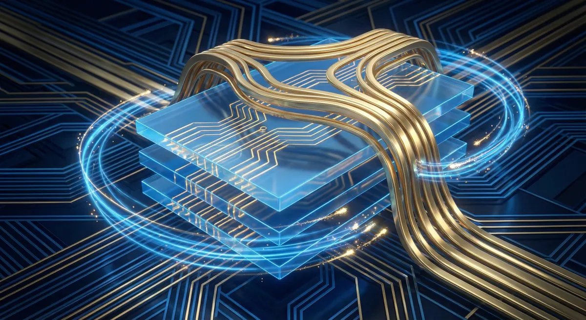
The A16 Revolution: Backside Power Delivery Arrives
While N2 represents a major leap forward, the real game-changer arrives in the second half of 2026 with TSMC's A16 node. Technically part of the 2nm family (sometimes described as 1.6nm in marketing materials), A16 introduces what TSMC calls "Super Power Rail"—the company's proprietary implementation of backside power delivery network (BSPDN) technology.
Traditional chip designs route both signals and power on the front side of the silicon, leading to congestion and inefficiency in complex, high-power designs. Backside power delivery physically separates power distribution to the rear of the wafer, freeing up the front side for denser signal routing and reducing voltage drop across the chip.
For AI accelerators—which feature massive parallel compute arrays consuming hundreds of watts—the benefits are substantial. TSMC claims A16 will deliver an additional 8-10% performance improvement over N2 in the same power envelope, or enable even greater power reductions for mobile and edge AI applications. Just as importantly, the technology enables higher transistor density and more complex chip designs, critical as models grow larger and more sophisticated.
Intel's competing 20A and 18A nodes (now rebranded as Intel 2 and Intel 1.8) also feature backside power delivery, and the company has been vocal about the advantages of its RibbonFET and PowerVia technologies. However, Intel's manufacturing challenges and limited external foundry customer base mean TSMC's A16 is likely to see broader adoption across the industry.
The Capacity Crunch: Billions at Stake
TSMC's 2026 capital expenditure budget stands at $52-56 billion, the highest in the company's history and a reflection of the massive buildout required to meet demand. The company is constructing new fab capacity in Taiwan while also working on 3nm production in Arizona—though 2nm technology will remain exclusive to Taiwan for the foreseeable future, a decision driven by both technical complexity and geopolitical considerations.
Industry reports indicate that N2 capacity is essentially sold out through late 2026, with A16 pre-orders already substantial despite the node not entering mass production until H2 2026. For TSMC's customers, securing allocation has become a strategic priority—and a competitive weapon.
Smaller fabless semiconductor companies without the purchasing power of Apple, NVIDIA, or AMD face a difficult calculus. They can pay premium pricing for limited capacity, accept delays in their product roadmaps, or consider alternative nodes that may not offer the same performance advantages. This dynamic is already reshaping the semiconductor supply chain, with second-tier chip designers exploring partnerships, capacity sharing arrangements, or even abandoning leading-edge designs entirely.
The Economics: Price Increases and Margin Pressure
TSMC has announced a 3-5% price increase for sub-5nm nodes in 2026, a move that reflects both the company's pricing power and the extraordinary costs associated with advanced process development. Wafer pricing for N2 and A16 is estimated at $16,000-20,000 per wafer, compared to roughly $13,000-15,000 for N3 nodes.
For customers, these increases are significant but largely unavoidable. The performance and efficiency gains from 2nm technology justify the premium for high-value products like flagship smartphones and AI accelerators, where silicon cost is a relatively small component of total system cost. However, the economics become more challenging for mid-range products or applications with thinner margins.
The rising cost of advanced nodes is also accelerating the bifurcation of the semiconductor industry. While leading-edge AI and mobile processors push toward 2nm and beyond, a growing number of chip designs are staying on mature nodes like 7nm, 12nm, or even larger geometries where performance requirements are less demanding and costs are dramatically lower.
The Strategic Implications: Process Leadership as Competitive Moat
TSMC's dominance in advanced logic manufacturing has become one of the most significant competitive moats in the technology industry. The company's ability to deliver working, high-yield processes at the leading edge—and to ramp production at scale—is a capability that Samsung and Intel have struggled to match despite massive investments.
For TSMC's customers, this creates both opportunity and risk. Access to the world's most advanced manufacturing enables products that competitors simply cannot match, a crucial advantage in markets like AI accelerators where performance directly translates to market share and revenue. However, dependence on a single supplier—particularly one located in a geopolitically sensitive region—creates supply chain vulnerability that keeps executives awake at night.
The U.S. government's CHIPS Act funding and efforts to build domestic semiconductor manufacturing capacity are a direct response to this concentration. However, replicating TSMC's capabilities in the United States or Europe will take years and tens of billions of additional investment, and even then may not match the yield, cost, or scale of TSMC's Taiwan operations.
Looking Ahead: The 1nm Era and Beyond
TSMC isn't resting on its 2nm achievements. The company has already announced its N1 (1nm class) technology for 2028-2029, with development work well underway. Early indications suggest N1 will build on the architectural innovations of A16, with further refinements to GAA transistors, backside power delivery, and 3D integration technologies.
NVIDIA is reportedly planning to be among the first adopters of the advanced nodes beyond A16, potentially targeting a 1.6nm or 1nm process for GPU architectures launching in 2028. As AI models continue to scale and demand for inference acceleration grows, access to the most advanced manufacturing will become even more critical.
The question facing the industry is whether demand can sustain the massive capital investments required to push Moore's Law forward. With wafer costs approaching $20,000 and design costs for leading-edge chips easily exceeding $500 million, the number of companies that can afford to play at the cutting edge is shrinking. Yet AI's insatiable appetite for compute suggests that for the foreseeable future, the investment will be worth it.
Conclusion: Silicon Scarcity in the AI Age
TSMC's 2nm production ramp represents both a technological triumph and a strategic chokepoint for the AI industry. As models grow larger and deployment accelerates, access to cutting-edge silicon has become as critical as access to data, algorithms, or engineering talent. The companies that secure their supply chains today—through long-term commitments, strategic partnerships, or in-house manufacturing—will have a decisive advantage in the AI race.
For TSMC, the challenge is managing extraordinary demand while maintaining the technological leadership that makes that demand possible. The company's $50+ billion capital budget, simultaneous fab ramps, and aggressive roadmap extending to 1nm and beyond suggest confidence that AI's growth will continue.
But in an industry where a single process node can take five years and $10 billion to develop, the margin for error is razor-thin. The 2nm capacity war is just beginning—and its outcome will shape the AI landscape for years to come.