Seventy-three billion dollars. That's more than the annual GDP of Luxembourg, more than the combined R&D spend of the top ten pharmaceutical companies, and the single largest capital expenditure commitment in Samsung Electronics' history. The target: overhaul its AI chip manufacturing and memory production fast enough to unseat SK Hynix as Nvidia's dominant HBM supplier — before the agentic AI wave crests and the window closes.
The HBM Arms Race
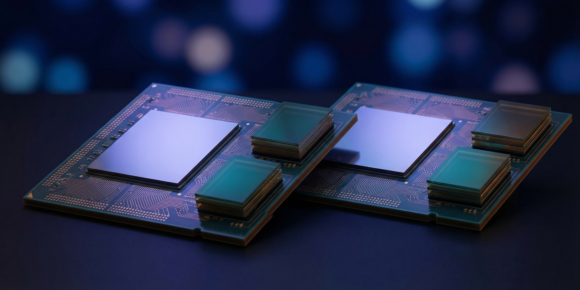
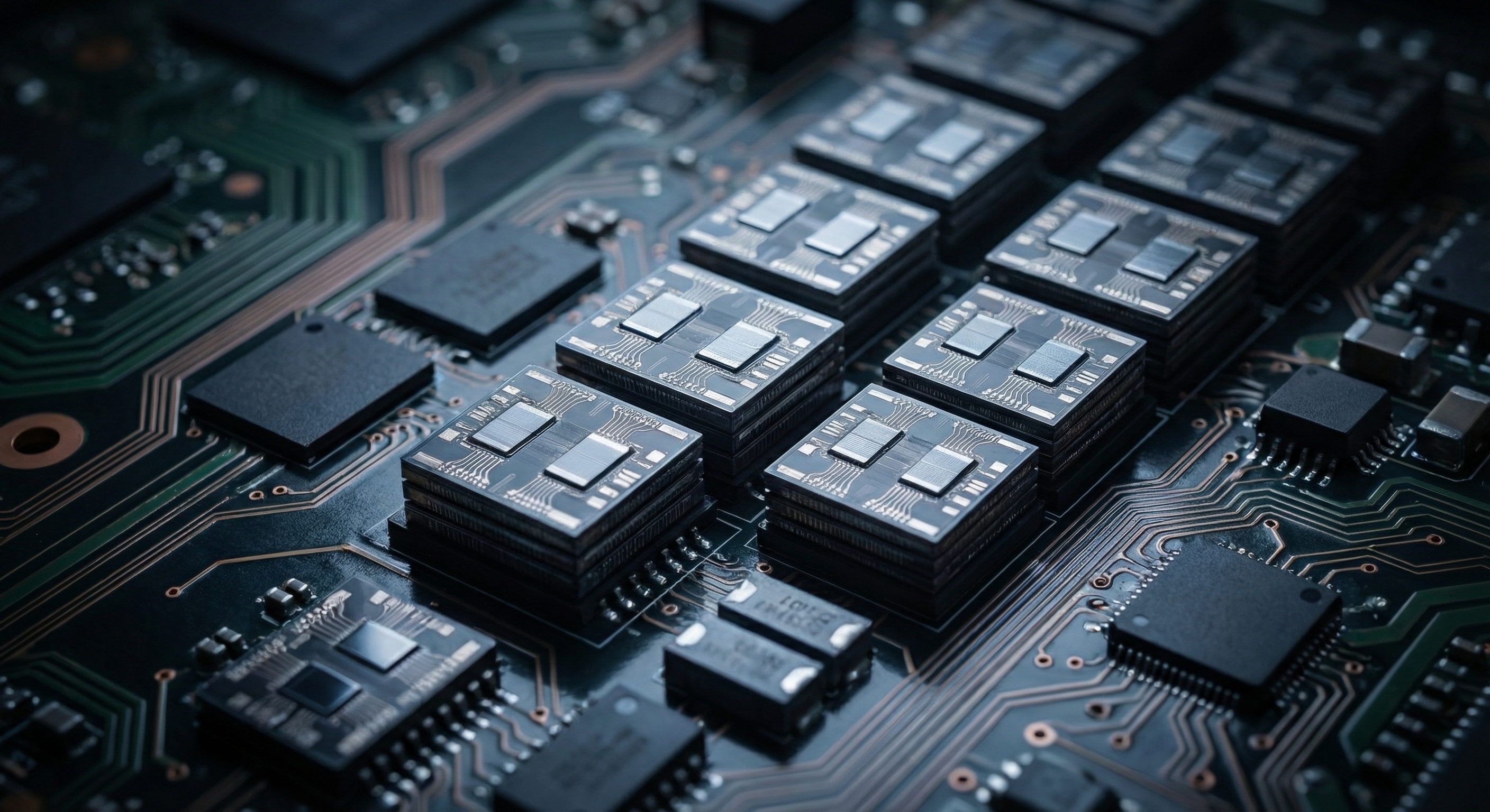
High Bandwidth Memory isn't a commodity. It's the architectural difference between an AI chip that can process massive neural network layers at speed and one that starves for data. HBM stacks multiple DRAM dies vertically and connects them with through-silicon vias, delivering memory bandwidth that conventional GDDR can't approach. Nvidia's flagship AI accelerators — H100, H200, and now the Vera Rubin platform — are built around HBM as a core design requirement, not an option.
For the past two years, SK Hynix has dominated Nvidia's HBM supply chain. The Korean rival was first to qualify HBM3E for Nvidia's Blackwell and H200 platforms, capturing the bulk of allocation in a market where supply was already oversubscribed. Samsung, despite being the world's largest semiconductor company by revenue, found itself in the unusual position of watching a competitor dictate the terms of the most important memory market in the industry's history.
The source of Samsung's setback was well-documented: HBM3E qualification delays in 2024 and 2025 kept its chips off Nvidia's approved vendor list for longer than expected. Quality control issues, yield challenges at the stacking process, and the sheer technical difficulty of next-generation HBM combined to cost Samsung the first-mover advantage it needed. SK Hynix shipped. Samsung waited for approval.
The $73 billion announcement is Samsung's answer to that delay — and its bet that the next cycle won't repeat the same outcome.
$73 Billion and a 22% Capex Jump
According to reporting by The Wall Street Journal, Samsung Electronics is committing over $73 billion in capital expenditure for 2026 — a 22% increase over its prior-year spending level. Co-CEO Jun Young-hyun explicitly framed the investment as a response to surging demand from agentic AI deployments, the next wave of AI architecture that requires sustained, high-throughput memory access rather than one-shot inference bursts.
The funds are directed across three priority areas. First: HBM production capacity expansion. Samsung is accelerating the buildout of dedicated HBM fabrication lines to increase its output of HBM3E and position itself for HBM4 volume production — the generation Nvidia has specified for the Vera Rubin Ultra platform. Second: advanced process R&D, including continued investment in Samsung's 2nm and sub-2nm gate-all-around (GAA) transistor architecture, which underpins the next generation of logic chips. Third: what Samsung describes as "future-oriented" sectors — a category that explicitly includes advanced robotics, tying the memory and chip story to the physical AI ecosystem.
To put the scale in context: $73 billion is roughly four times Samsung's annual net profit in a good year. It's a commitment that signals the company views the AI chip market not as a cyclical opportunity but as a structural shift that warrants sustained, aggressive investment regardless of near-term margin pressure.
Agentic AI Changes the Memory Calculus
Jun Young-hyun's framing around agentic AI is analytically important, not just marketing. Traditional inference workloads — a user sends a query, the model responds — are relatively predictable in their memory demands. A single forward pass through a large language model requires loading weights into memory, performing matrix operations, and returning a result. The memory traffic is intense but bounded.
Agentic AI operates differently. An agent tasked with researching a topic, writing a report, executing code, and revising its work over an extended session must maintain much larger working state in memory, make many more sequential inference calls, and orchestrate multiple tool interactions simultaneously. The memory bandwidth requirements for agentic workloads are structurally higher — and they scale with the length and complexity of the task, not just the size of the model.
This is why memory architects are watching the agentic transition carefully. As AI infrastructure providers scale from single-query inference to multi-step agentic pipelines, the demand profile for HBM changes. More bandwidth, more sustained utilization, longer periods of continuous operation. The memory supplier who can deliver that profile reliably — and at scale — wins contracts that compound over years, not quarters.
Samsung's bet is that the agentic wave justifies a $73 billion acceleration. If the demand forecast is correct, the company that captures HBM4 supply leadership for Nvidia's next platform will be positioned to dominate memory supply through at least 2028.
SK Hynix Isn't Standing Still
Samsung's challenge is real, but it arrives against a competitor that's been investing aggressively in its own position. SK Hynix currently supplies the dominant share of HBM to Nvidia and has already announced its own HBM4 development roadmap. The company's manufacturing yield on HBM3E has reportedly been strong enough to sustain Nvidia's Blackwell ramp at scale — which is precisely the track record Samsung needs to replicate.
HBM4 raises the technical stakes further. The next-generation standard introduces a wider interface bus, higher per-die capacity, and tighter integration requirements with the logic chip — including a potential shift toward base-die logic that blurs the line between memory and compute. Both Samsung and SK Hynix have already locked up Nvidia's Vera Rubin HBM4 allocations, cutting Micron from the flagship supply cycle entirely — but allocation and qualification are different things. Samsung has to demonstrate that its HBM4 production meets Nvidia's quality and yield requirements consistently enough to justify a larger share of the order book.
The competitive dynamic is essentially this: Samsung has the manufacturing scale and the R&D depth to challenge SK Hynix. What it needs to close the gap is the quality consistency and qualification speed to match a rival that has spent two years building trust with the world's most important AI chip customer.
The Robotics Wildcard
One of the more striking elements of Samsung's announcement is its explicit inclusion of advanced robotics in the investment thesis. While most coverage has focused on HBM and AI accelerator memory, the robotics allocation signals that Samsung sees its chip investment as part of a broader physical AI play.
The connection makes sense from a systems perspective. Physical AI — robots, autonomous vehicles, edge inference devices — requires specialized memory architectures that are distinct from data center HBM. Low-power, low-latency memory for edge inference. High-reliability DRAM for safety-critical systems. Specialized NAND for the vast amounts of sensor data that robotic systems must store and retrieve. Samsung, as a diversified memory company, has products that span the full stack from server HBM to embedded mobile DRAM.
The robotics allocation also hedges the investment thesis. If the data center AI cycle slows or consolidates around fewer suppliers, physical AI represents an independent demand vector that grows as humanoid robots and autonomous systems move toward mass deployment. Samsung is not just betting on Nvidia's HBM roadmap — it's betting on the entire hardware stack that physical AI will require over the next decade.
What Comes Next
The immediate question is HBM4 qualification. Samsung must demonstrate to Nvidia that its HBM4 production — presumably targeting the Vera Rubin Ultra and post-Rubin platforms — meets the yield, bandwidth, and reliability specifications required for inclusion in Nvidia's supply chain at meaningful scale. This is a technical milestone, not a financial one, and it can't be accelerated simply by spending more money. Process optimization takes time.
Longer term, the $73 billion commitment positions Samsung for the HBM5 cycle and beyond. The company has already committed to its 2nm GAA process node as a production capability by 2026, which gives it the logic fabrication foundation to develop the base-die architectures that next-generation HBM will require. If that development cadence stays on schedule, Samsung enters the HBM5 competition with both the manufacturing capacity and the process technology to compete on equal footing.
The wildcard is geopolitical. Samsung's primary manufacturing facilities are in South Korea and Texas — but its supply chain has exposure to the ongoing US-China trade tensions that have reshaped chip industry economics over the past three years. Any further tightening of export controls, equipment restrictions, or tariff regimes could complicate Samsung's capacity expansion plans, particularly for advanced packaging equipment sourced from ASML and other Western suppliers.
A $73 Billion Question With No Guaranteed Answer
The AI chip supply chain is not a commodity market. It is an oligopoly in which three companies — Samsung, SK Hynix, and Micron — control the entire global supply of HBM, and in which a single customer (Nvidia) accounts for the majority of demand at the premium end of the market. In that structure, the difference between first and second place in Nvidia's supply chain isn't measured in market share points. It's measured in billions of dollars of annual revenue and the strategic leverage that comes with being the preferred supplier to the infrastructure that powers AI.
Samsung's $73 billion bet is, at its core, a wager that the AI wave is real, durable, and worth the most aggressive capital deployment in the company's history. The demand signal from agentic AI supports that wager. The competitive pressure from SK Hynix makes it necessary. And the qualification math — the technical work of getting HBM4 chips into Nvidia's approval queue and out the other side at volume — will determine whether the investment pays off or becomes the most expensive second-place finish in semiconductor history.
The money is committed. The technical work begins now.