On March 14, Elon Musk posted two words on X that set the semiconductor industry on edge: "Terafab Project launches in 7 days." No technical specs. No press release. Just a countdown to what could be the most disruptive move in chip manufacturing since TSMC opened its first fab in Taiwan. Tesla's Terafab — a $25 billion vertically integrated AI chip fabrication facility — is scheduled to launch March 21, and the industry is still scrambling to fully comprehend what it means.
What Terafab Actually Is
Tesla first publicly confirmed Terafab on its January 28, 2026 earnings call. Musk told investors the company had concluded that it needed its own chip fabrication capability to avoid a supply constraint projected to materialize within three to four years. The numbers he cited were not incremental: Terafab is designed to produce between 100 and 200 billion custom AI and memory chips per year, with an initial target of 100,000 wafer starts per month and a stated ambition to scale toward one million — a figure that represents roughly 70% of TSMC's current total output from a single US facility.
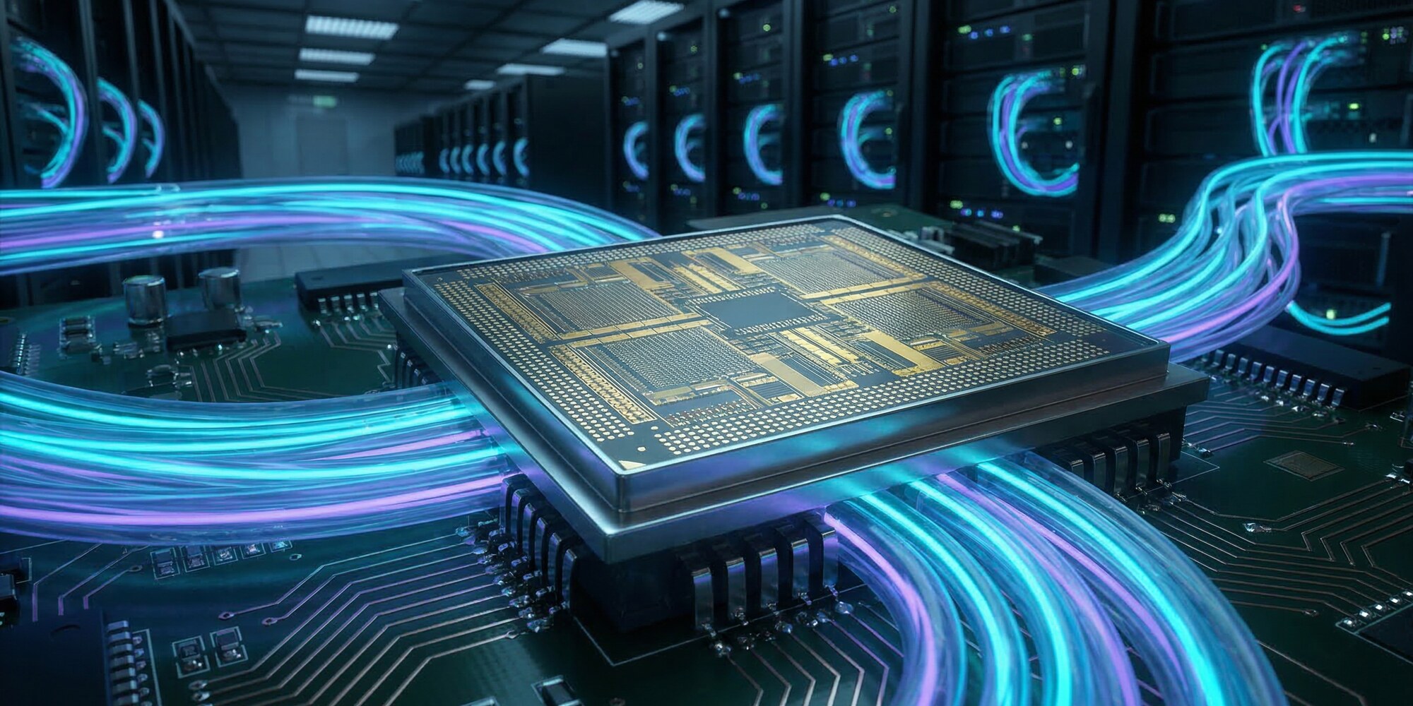
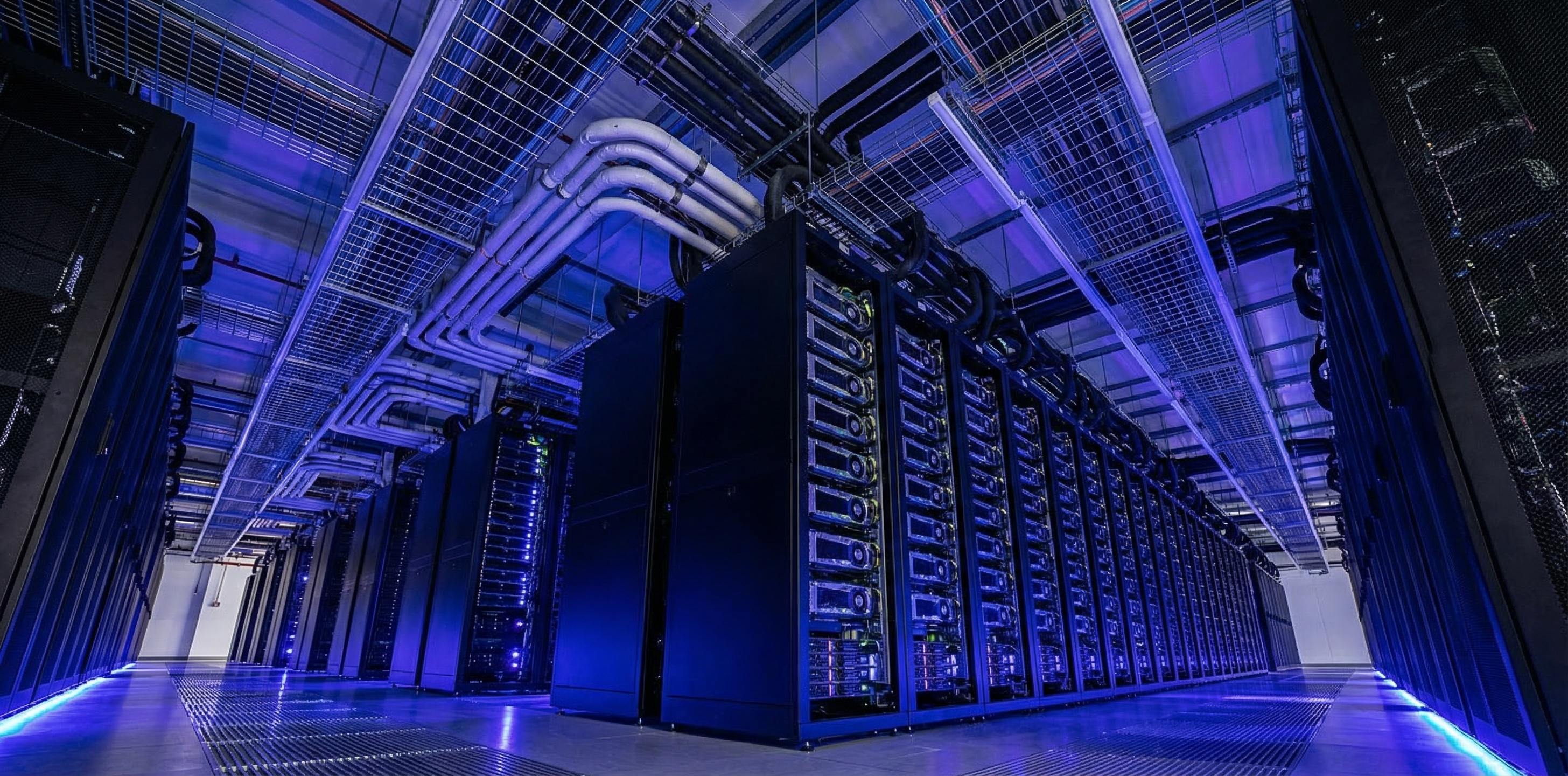
The architecture of Terafab is what separates it from any existing US chip manufacturing effort. Unlike conventional fabs that handle one layer of the stack, Terafab is designed to combine logic processing, memory storage, and advanced packaging under one roof — vertically integrated chip manufacturing at a scale that no private company outside Taiwan and South Korea currently operates. Tesla is targeting 2 nanometre process technology, currently the most advanced node in commercial production anywhere in the world.
The estimated cost of $25 billion sits outside Tesla's stated 2026 capital expenditure plan of $20 billion, which CFO Vaibhav Taneja acknowledged on the earnings call does not yet fully incorporate Terafab's total outlay. In other words, the headline capex number investors have been modeling may already be understated by a significant margin.
The Supply Chain Problem Driving This
The strategic logic behind Terafab is not difficult to follow. Tesla's autonomous vehicle ambitions, its Cybercab robotaxi program, and its Optimus humanoid robot line all require volumes of custom AI silicon that existing external suppliers cannot commit to on Tesla's timelines. Musk has been explicit about this for over a year. "Even when we extrapolate the best-case scenario for chip production from our suppliers, it's still not enough," he said at Tesla's annual meeting last year.
TSMC and Samsung are Tesla's current chip production partners. Both are running at or near capacity across their most advanced nodes, facing competing demand from Apple, NVIDIA, AMD, Google, and now a growing field of hyperscaler custom silicon programs. The 2nm capacity war at TSMC has been one of the defining supply stories of 2026 — with major customers locked into allocations negotiated months or years in advance. For a company projecting the chip volumes that Optimus alone would require at scale, that is a structural problem with no easy fix inside the existing ecosystem.
Tesla's fifth-generation AI chip, AI5, is among the first products Terafab is designed to produce. Small-batch production is expected in 2026, with volume production projected for 2027. AI5 powers Full Self-Driving software, the Cybercab platform, and the Optimus neural stack — making it the single most important piece of silicon in Tesla's product roadmap.
The xAI Dimension
Terafab is not purely a Tesla story. Musk has described its scope as explicitly encompassing chips for xAI — both for Dojo, Tesla's in-house supercomputer used to train Full Self-Driving models, and for xAI's Grok model training infrastructure. The Memphis supercluster that xAI currently operates is already one of the largest GPU clusters in existence. Tom's Hardware has reported that Musk is expanding xAI's training capacity to a monstrous 2 gigawatts with a third building at the Memphis site. Terafab is the supply chain that would make the next generation of that infrastructure independent of external suppliers entirely.
The convergence of Tesla's autonomy compute and xAI's model training under a shared internal silicon supply chain is a vertical integration play with few precedents in modern tech. It is conceptually similar to Apple's transition away from Intel — but executed at a far larger scale and across two major AI-adjacent businesses simultaneously.
The Texas Infrastructure Signal
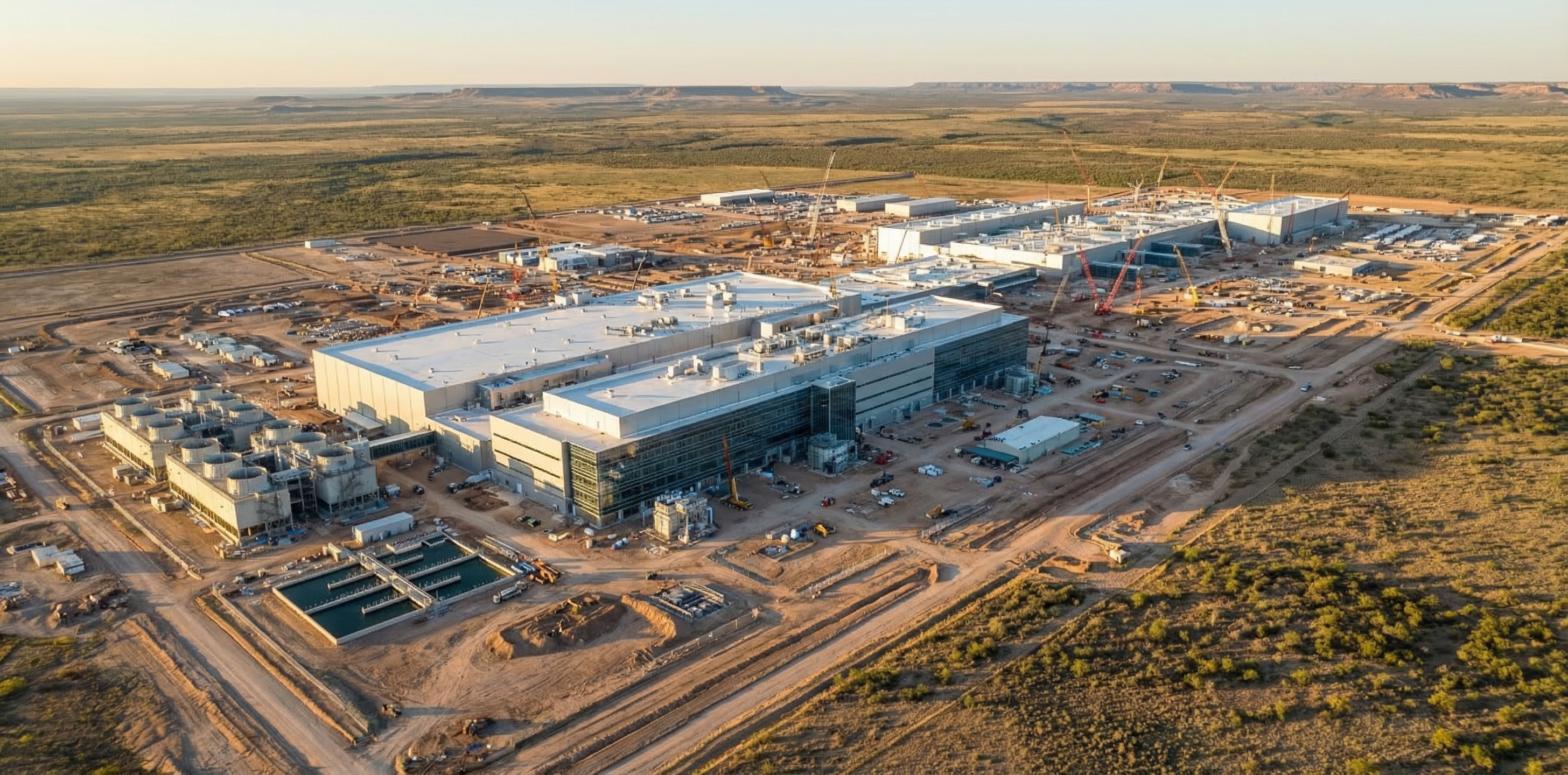
While Tesla has not officially confirmed Terafab's physical location, early signs of its construction have already emerged. In late 2025, Tesla quietly advanced a fan-out panel-level packaging (FOPLP) plant in Texas, targeting volume production by Q3 2026. Fan-out panel-level packaging is a critical enabling technology for advanced AI chip assembly — allowing chiplets and dies to be combined at scale without the yield limitations of traditional package substrates. That Texas facility, paired with Terafab's broader vertical integration mandate, points strongly toward Texas as the site for the core fab, likely co-located with or adjacent to Tesla's existing Gigafactory Texas presence in Austin.
The broader US chip manufacturing expansion provides context. Samsung's Taylor, Texas fab is on track for risk production in 2026. TSMC's Arizona facilities are ramping toward their own output targets. Intel has been attempting a foundry revival with its 18A process node. Tesla would be entering a US semiconductor manufacturing landscape that is more capable than at any point in a generation — but still nowhere near the depth of Taiwan's ecosystem. Musk has publicly discussed potential collaboration with Intel, though Reuters confirmed no deal has been signed.
What "Launches in 7 Days" Actually Means
The phrase "Terafab Project launches in 7 days" is not unambiguous. A chip fab does not flip a switch and begin producing 2nm silicon — construction, tooling, and process qualification for a greenfield fab takes years. What March 21 almost certainly represents is either a formal groundbreaking ceremony, the official announcement of the project's structure, location, and partnership details, or the launch of the corporate entity or procurement process that will execute Terafab's buildout.
Analysts tracking the story have noted that the term "launches" in Musk's vocabulary has historically referred to the official public initiation of a project — not its completion. SpaceX "launched" the Starship program years before a full-stack orbital flight. Tesla "launched" the Semi before factory deliveries. March 21 is the beginning of Terafab's public chapter, not the moment it starts printing chips.
That said, the fact that Musk felt confident enough to set a specific seven-day countdown implies that at least the structural components — location selection, key partnership terms, anchor technology agreements, and initial capex commitment — are sufficiently advanced to withstand public scrutiny. This is not a vaporware announcement. The FOPLP work in Texas, the AI5 chip design timeline, and the supply constraint projections Musk cited on the earnings call all point to a project with genuine engineering momentum behind it.
The Industry Implications
If Terafab delivers on even a fraction of its stated ambitions, the implications for the global semiconductor supply chain are profound. A single US private facility targeting 70% of TSMC's current output would represent a step-change in domestic chip production capacity that no CHIPS Act subsidy package has come close to achieving. It would meaningfully reduce Tesla and xAI's dependence on Taiwanese and South Korean foundries — a geopolitical risk consideration that has been a persistent undercurrent in every major AI infrastructure investment conversation of the past three years.
For TSMC specifically, the prospect of a major customer building out internal capacity at Terafab scale is the kind of demand signal that reshapes long-range capacity planning. Broadcom's recent moves with custom silicon and Meta's aggressive MTIA chip roadmap have already signaled that the hyperscale custom silicon trend is accelerating. Terafab adds a new dimension: a vertically integrated fab, not just a chip design effort outsourced to foundry partners.
The competitive pressure on NVIDIA is also worth noting. Tesla's AI5 chip is not a data center GPU — it is a purpose-built autonomy and robotics processor optimized for Tesla's specific inference workloads. But as xAI's training compute ambitions grow, and as Terafab's scope expands to encompass Grok training silicon, the question of whether internally produced accelerators could eventually displace some portion of third-party GPU spend becomes relevant. NVIDIA's GTC 2026 roadmap remains the dominant force in AI compute architecture — but the number of entities capable of building compelling alternatives at scale is growing.
The Uncertainty That Remains
The ambition is clear. The execution risk is substantial. Building a 2nm chip fab from scratch is among the most technically demanding industrial projects a company can undertake. TSMC took decades to reach its current level of process maturity. Samsung has poured hundreds of billions into foundry infrastructure and is still working through yield challenges at leading-edge nodes. Intel's 18A recovery has moved faster than many expected but is still in the early stages of commercial validation.
Tesla has no foundry history. Its chip design capability, while impressive for an automotive company, is not in the same league as the teams at Apple, Google, or NVIDIA that have developed complex silicon over decades. The 2nm target is not a guaranteed destination — it is a stated ambition for a facility that does not yet exist in its final form.
What March 21 will clarify is how much of the hard work has already been done in private, and how much of the Terafab story is still in the projection phase. The seven-day countdown is, above all else, a commitment to be held accountable. The industry will be watching.